← All projects

Analog / Electronics

Analog Circuit Design & Characterization

Built, measured, and simulated analog circuits across op amps, BJT amplifiers, diodes, and MOSFET/CMOS devices in EECE 2413.

Analog CircuitsPSpiceBreadboardingCircuit Testing
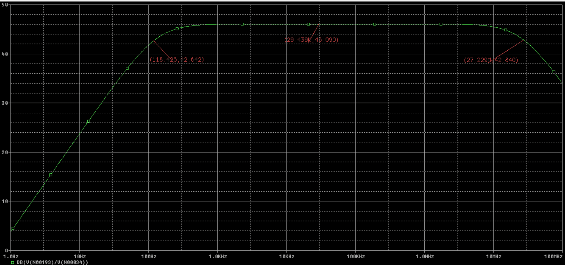
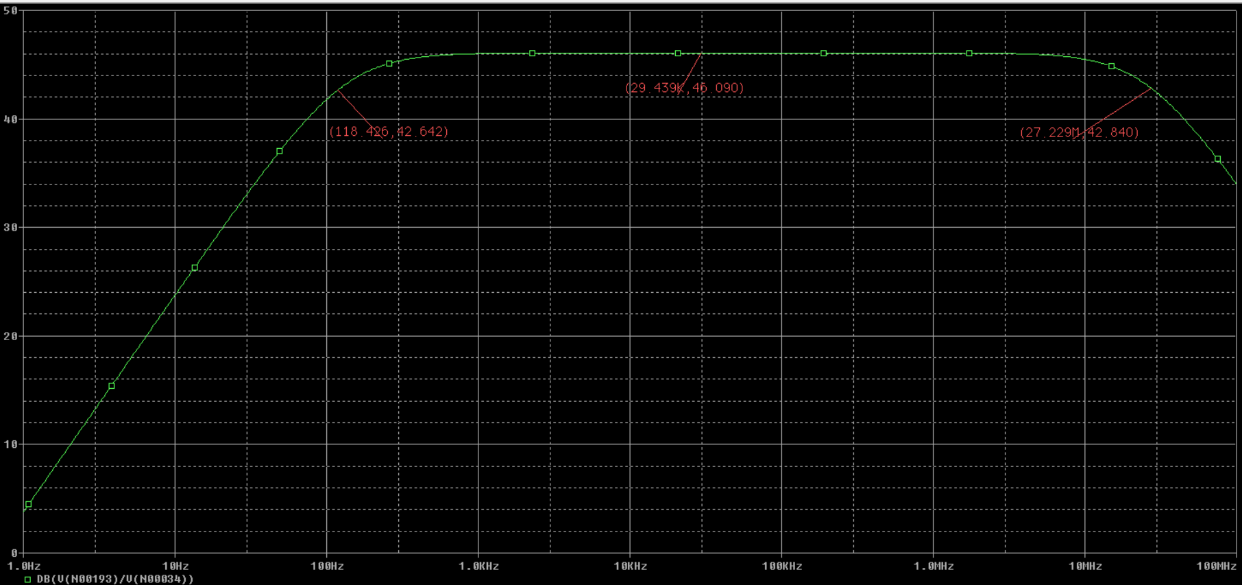
Original PSpice AC sweep from the BJT amplifier lab report
Original PSpice simulation · Lab 4

01 / Overview

Project at a glance.

Five electronics labs connect design calculations, circuit construction, simulation, and measurement across amplifiers and semiconductor devices.

5 reportsElectronics investigations
≈20BJT target gain
8–12 VSupply investigation
PSpiceSimulation comparison

02 / System approach

From design to measurement.

A repeatable investigation process connects each design to its simulated and measured behavior.

  1. 01Calculate & design
  2. 02Simulate
  3. 03Build & measure
  4. 04Compare & refine

Electronics from theory to measurement

Completed in EECE 2412, Fundamentals of Electronics, and EECE 2413, Lab for EECE 2412, at Northeastern University in Spring 2026. The lecture covers semiconductor devices, biasing, switching, CMOS logic, small-signal analysis, and PSpice modeling; the lab reinforces these topics through circuit construction and practical measurements. Five reports document hands-on circuit construction, measurements, calculations, and PSpice simulations across amplifiers and semiconductor devices.

BJT amplifier design

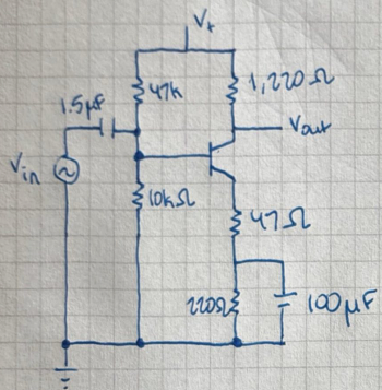
Lab 4 investigated common-emitter amplifier gain, clipping, supply sensitivity, and frequency response. Emitter resistance improved stability while reducing gain; a bypass capacitor increased AC gain while retaining the DC bias network. The report documents a final amplifier targeting a gain of approximately 20, with measured gain remaining within the required range across supplies from 8 V to 12 V.

Op-amp microphone amplifier

Lab 1 explored LM741 inverting and non-inverting circuits, including gain, phase shift, clipping, slew rate, and load effects. The report gives a measured gain magnitude of 11.19 against a theoretical value of 10 for the inverting circuit, and 102.5 against 101 for the non-inverting amplifier. PSpice simulations supported comparison with the experimental behavior.

MOSFET and CMOS characterization

Lab 5 measured inverter voltage-transfer characteristics, extracted device parameters, and examined switching and amplification. The report describes a sharper transition and reduced power dissipation for the CMOS inverter compared with the resistor-loaded MOSFET circuit. It also documents differences between the simplified PSpice transistor model and the measured device.

Smaller circuit applications

Lab 2 applied diode and Zener behavior to a staged LED voltage indicator. Lab 3 explored BJT operating regions and a photocell-based automatic night light, with a timing capacitor used to avoid flicker.

A repeatable design and verification process

  1. Measure the components and operating point

    The reports begin with bench measurements rather than ideal component values alone. Resistor values and transistor node voltages support calculations of current, bias conditions, and expected gain.

  2. Compare predicted and observed behavior

    Oscilloscope measurements test gain, phase, clipping, and frequency response. PSpice operating-point, transient, AC-sweep, and DC-sweep analyses provide separate model-based comparisons.

  3. Revise for practical constraints

    The amplifier work adds emitter feedback for stability and a bypass capacitor to recover AC gain. The night-light design adds a timing capacitor to prevent flickering. These changes address observed system behavior rather than only matching an ideal calculation.

Selected evidence across EECE 2413 Labs 1–5
InvestigationReported evidence
Op-amp gain and loading · Lab 1Measured gain magnitudes of 11.19 and 102.5 against targets of 10 and 101. Replacing the high-impedance piezoelectric load with an 8 Ω speaker produced no audible output.
LED voltage indicator · Lab 2Designed staged red/yellow/green activation for input bands of 0–2 V, 2–8 V, 8–17 V, and 17–24 V; the report concludes the design met its specifications.
Automatic night light · Lab 3Reported photocell resistance of 2.65 kΩ in light and 175 kΩ in darkness. A 100 µF timing capacitor delayed the response by roughly one second and prevented brief light interruptions from causing flicker.
Stable BJT amplifier · Lab 4The final design targeted gain near 20 and reportedly stayed within the required gain range across 8–12 V supplies.
MOSFET/CMOS comparison · Lab 5Measured transfer characteristics showed a sharper CMOS transition. The simplified PSpice MOSFET model differed from the physical device, including a simulated low-output level near 4 V.

Applying transistor behavior

A light-sensitive switch

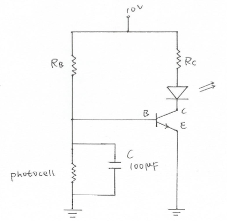
The Lab 3 night light uses a CdS photocell in the transistor’s base-bias network. In darkness, its higher resistance allows the transistor to turn on and drive the LED. Illumination lowers the resistance and turns the LED off. The capacitor slows the base-voltage response so the light condition must persist before the output changes.

Original automatic night-light schematic with 10 V supply, transistor, LED, photocell and 100 microfarad timing capacitor
Original Lab 3 design schematic · Open full size ↗

From inverter characteristics to logic

Lab 5 used CD4007 MOSFETs to examine resistor-loaded NMOS and complementary CMOS inverter behavior. The design portion then implemented a three-input OR function using a three-input NOR followed by an inverter, with push-button inputs. This connects device-level characterization to digital logic construction.

Original design and simulation

These figures come from the Lab 4 report. The frequency-response plot is a simulation result.

Original hand-drawn BJT amplifier schematic with bias network, split emitter resistor, and bypass capacitor
Original amplifier schematic · Open full size ↗
Original PSpice AC sweep from the BJT amplifier lab report
PSpice AC sweep · Open full size ↗

Design tradeoffs and further details

Across these labs, measurements and simulations reveal the practical effects of component behavior, loading, operating point, and frequency. The amplifier investigation highlights the tradeoff between gain and stability, while the MOSFET investigation demonstrates why simulation models must be compared with physical measurements.

Individual contribution

To add: individual responsibilities and team context.

Gain versus stability

Emitter resistance introduces negative feedback that stabilizes the BJT amplifier but reduces gain. Bypassing part of that resistance increases AC gain while preserving the DC bias network.

Models versus measurements

Loading and component behavior affect practical performance. The Lab 1 speaker substitution exposed output-drive limitations, and Lab 5 showed why a simplified transistor model must be checked against the measured device.

Project resources

To add: public repository, report, and demonstration links.

Source material

Based on Justin Ho’s final EECE 2413 Lab 1–5 reports from Spring 2026. The original schematic and AC sweep shown here come from Lab 4; the AC sweep is a simulation result, not a measured hardware trace.