Instruction flow
PC Logic feeds Instruction Memory. The Mapper separates instruction fields before they reach the Instruction Decoder.
FPGA / Digital Design
Designed and implemented a single-cycle processor on a Xilinx Zynq FPGA, integrating the datapath, control logic, register file, memory, instruction decoding, and branching.
01 / Overview
A single-cycle datapath connects instruction decoding, register access, arithmetic, memory, and branching on an FPGA.
02 / System approach
A simplified view of the functional path. Original artifacts and detailed evidence follow below.
This individual project connects instruction decoding, register access, arithmetic, memory, and branching in a RISC-V-style single-cycle processor. The build progressed through a series of SystemVerilog labs, turning separately tested components into a connected datapath.
Xilinx Zynq FPGA · SystemVerilog · Vivado · Virtual I/O
The Lab 1 hardware photograph identifies the board as a TUL PYNQ-Z2 with a Zynq-7020.
Summer 2025 · EECE 2322: Fundamentals of Digital Design and Computer Organization · EECE 2323: Lab for EECE 2322 · Professor Julius Marpaung.
I completed all implementation and report work, including the earlier lab exercises that built toward the processor.
EECE 2322 connects number systems, combinational and sequential logic, instruction-set architecture, and processor construction. EECE 2323 applies those ideas through FPGA implementation, simulation, and hardware testing.
The reports document the progression from a 16-bit adder to an ALU, register-file integration, and data memory. The final datapath diagram adds instruction flow and control. This is a custom educational RISC-V-style design; standard RISC-V ISA compatibility is not established by the supplied material.
The original diagram shows the instruction, data, and control connections, including 16-bit instruction and data labels.
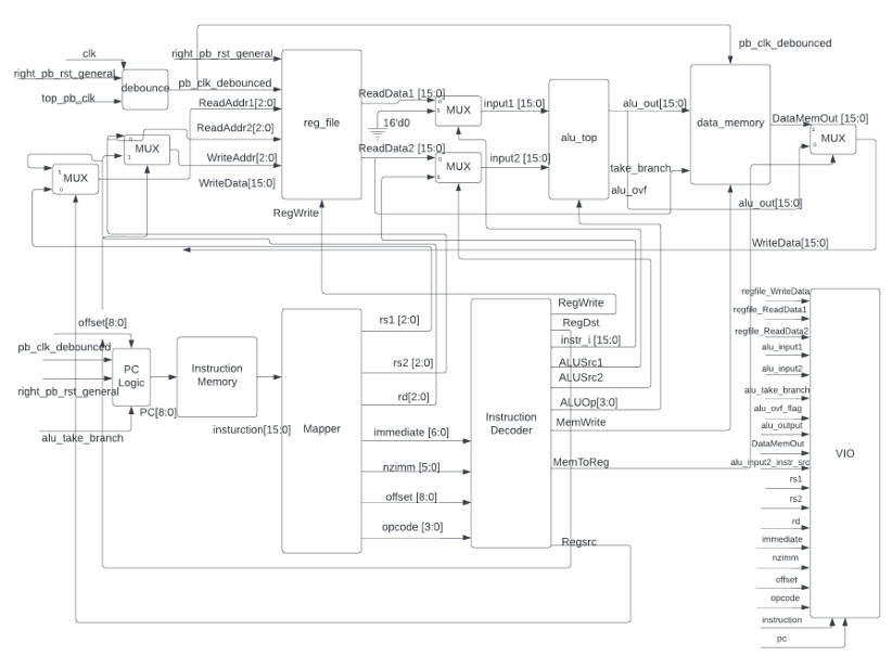
PC Logic feeds Instruction Memory. The Mapper separates instruction fields before they reach the Instruction Decoder.
The decoder exposes RegWrite, RegDst, ALUSrc1, ALUSrc2, ALUOp, MemWrite, MemToReg, and Regsrc to coordinate the datapath.
Two register read outputs feed operand-selection multiplexers before the ALU. A write-data path returns results to the register file.
The ALU supplies the data-memory address. A multiplexer selects the ALU result or memory output for register write-back.
The ALU exposes take_branch and overflow signals. The branch signal feeds the PC logic.
Debounce logic supplies a push-button clock signal, while Virtual I/O exposes internal signals for control and observation.
Lab 1 implemented a two-input, 16-bit adder in SystemVerilog. The sum is limited to 16 bits, while a separate overflow flag detects when same-sign operands produce a result with the opposite sign. A testbench exercised supplied vectors and additional all-zero/all-one patterns before hardware testing.
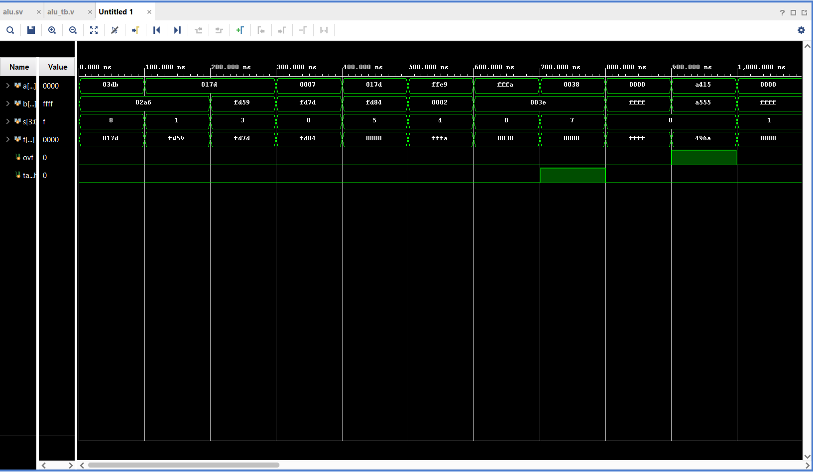
Lab 2 expanded the arithmetic block into an ALU with two signed 16-bit operands and a 4-bit operation selector. The source code implements addition, bitwise inversion, AND, OR, arithmetic right shift, left shift, zero/nonzero branch conditions, and XOR. A default case sets the result and flags to zero for unassigned select codes.
Overflow is calculated for addition. Branch conditions drive a separate take_branch output, separating control information from the arithmetic result.
Lab 3 integrated an eight-register, 16-bit register file with the ALU and two multiplexers. The source uses clocked writes with a write-enable signal, reset-to-zero behavior, and combinational reads. The multiplexers choose between register values, zero, and an immediate operand.
The integration test writes 12 and 17 into registers 2 and 3, reads them back, and routes both values through the ALU to produce 29.
Lab 4 added a Vivado memory IP core to a supplied top-level module and aligned its connections with the datapath. The ALU provides the memory address, a register output supplies write data, and a write-back multiplexer selects either the ALU result or memory output.
The VIO configuration was extended to control register writes, operand selection, memory writes, addresses, and write-back selection. Hardware sequences then exercised register-to-memory stores and memory-to-register loads.
The complete diagram connects PC logic, instruction memory, a Mapper, and an Instruction Decoder to the datapath controls. It also includes a branch-feedback path and debounced push-button clocking.
The final instruction encoding, decoder implementation, program examples, and complete-processor demonstration remain to be documented.
Labs 1–2 describe SystemVerilog testbenches, Vivado waveforms, and checks on the PYNQ board. Lab 3 documents register-file/ALU integration in simulation. Lab 4 explicitly used hardware testing without a separate simulation run.
| Stage | Method and scope | Reported outcome |
|---|---|---|
| 16-bit adder · Lab 1 | Expected sums and signed-overflow flags compared with Vivado simulation and PYNQ hardware outputs. | Reported matching results |
| ALU · Lab 2 | Testbench vectors cover operation selection, shifts, overflow, branch conditions, and unassigned select codes; hardware checks use VIO. | Reported matching results |
| Register file + ALU · Lab 3 | Write 12 and 17 to registers 2 and 3, then read both operands and add them. | Reported simulation result: 29 |
| Data memory · Lab 4 | Hardware sequences write values to registers, store them in memory, load them back, and add the retrieved operands. | Reported correct hardware outputs |
| Complete processor | The original diagram documents instruction decoding and PC/branch connections. | Full-program execution evidence to add |
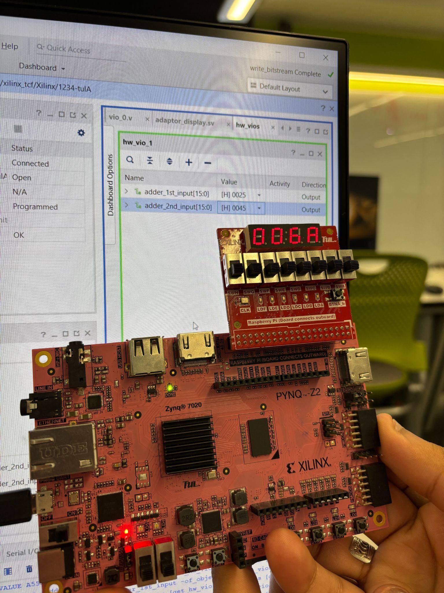
The photograph shows both operands entered through Vivado VIO and the sum displayed on the board’s attached display. The report lists an overflow flag of 0 for this case.
A second reported vector, 0xA415 + 0xA555, produces 0x496A with overflow set to 1. Together, these cases illustrate checking both the numeric output and the signed-overflow flag.
These are adder-stage results. They do not establish execution of a full instruction program.
Two 16-bit operands already require 32 input bits. The reports explain that the board did not provide enough physical inputs for these tests, so Vivado Virtual I/O supplied full-width values and exposed internal controls.
The ALU needed correct behavior for more than its result bus. The implementation separates signed-overflow detection, arithmetic shifting, and branch-condition outputs, with test vectors covering operation selection and unassigned codes.
Register writes, ALU operand selection, memory addresses, and write-back selection must agree. Lab 4 addressed this with explicit control-value sequences for storing and retrieving values, followed by hardware checks.
The reports trace a progression from a single arithmetic function to a connected system. Their conclusions emphasize the value of reusing the ALU across operations and extending the datapath with memory to store and retrieve data.
The reports conclude that the adder and ALU matched expected outputs, demonstrate a register-file/ALU addition in simulation, and report correct data-memory hardware behavior. Full-processor program traces, timing, and resource utilization are still needed to document the final system’s verification.
Based on the EECE 2323 Lab 1 report dated July 7, 2025; Lab 2 dated July 8, 2025; the Lab 3 register-file integration report; Lab 4 dated July 23, 2025; and the original processor datapath. Implementation details follow the included source code where the report prose differs. The scene at the top of this page is illustrative; the waveform and hardware photograph above are original report assets.